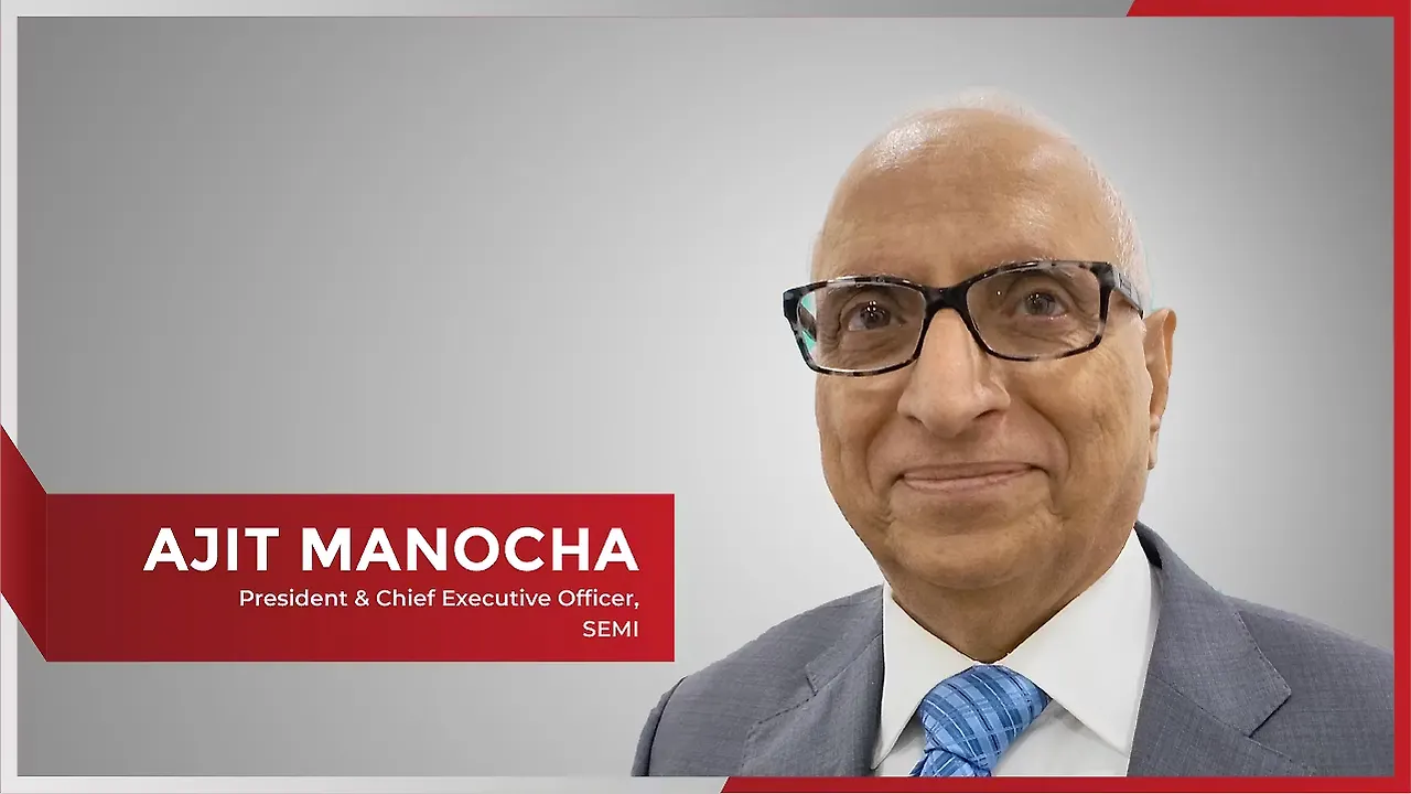
Ajit Manocha is the President and CEO of SEMI, the global industry association serving the semiconductor and electronics manufacturing and design supply chain. Manocha was formerly CEO at GlobalFoundries. Prior to this, he held the role of Executive VP of worldwide operations at Spansion and earlier served as Executive VP and chief manufacturing officer at Philips Semiconductors. He began his career at AT&T Bell Laboratories as a research scientist and was granted more than a dozen patents related to semiconductor manufacturing processes that served as the foundation for modern microelectronics manufacturing.
A few days before SEMICON India 2024, the Minister for Commerce, Industry, and IT said India could soon become the world's largest semiconductor manufacturer. What’s your view on this?
India has the potential to become the largest semiconductor manufacturer, but success depends on key factors. It starts with a clear vision, which India now has, followed by the right strategies and policies. For the first time in decades, the government's semiconductor policy, introduced in the past three years, has been thoroughly planned and executed.
Previously, I was hesitant about India entering this space without a clear framework, but the 2021 policy changed my outlook. The progress, especially by the Ministry of IT, has been impressive. Before 2022, India had no semiconductor fabs, yet within two years, five fabs have been announced, marking a significant achievement.
Are there any missing links?What’s missing is the development of a robust parts ecosystem. At SEMI, we excel in enabling ecosystems in different countries, and I’ve personally committed to bringing this crucial component to India. SEMICON India 2024, the first global semiconductor conference held in the country, has laid the foundation; but it’s only the beginning. However, we had more than 100 CEOs and CXOs in attendance, followed by a select group who participated in a roundtable with the Prime Minister. The consensus was unanimous: this is the right time for global partners to engage with India as a trusted player in the electronics and semiconductor supply chain. We are on the right path; now it’s time for execution.
What challenges does India face in kick-starting semiconductor manufacturing?
The semiconductor industry is one of the most complex and intricate in the world. Speaking from my own experience of building two greenfield fabs—one in Madrid, Spain, and another in Malta, New York—I can tell you that creating a semiconductor manufacturing ecosystem is far from trivial. Both locations initially lacked the necessary infrastructure and support industries, and building that ecosystem required tremendous coordination and collaboration across multiple sectors.
The success of a fab depends on support from industries ranging from construction to equipment suppliers, materials companies, design firms, etc. Every component must align perfectly, and there is no room for delays or errors. When you're dealing with a $10 billion investment, where $8 billion of that goes into equipment, even a minor failure can shut down the entire operation. You can't skip steps or work around a malfunction—everything happens in a precise sequence, and every stage depends on the flawless functioning of the previous one.

What are the risks involved in manufacturing?
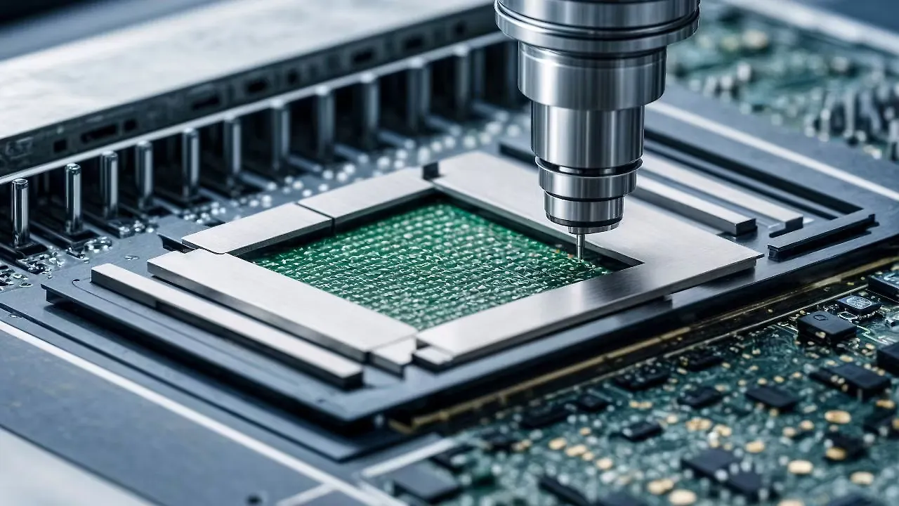
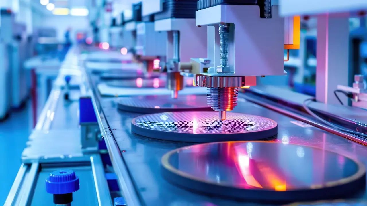
The manufacturing process is highly sequential, with lead times for a wafer in the fab ranging from six to eight weeks. A single mistake means starting from scratch, with the potential to lose millions of dollars in the process. The complexity begins with the raw material—typically a silicon substrate—on which circuits are printed, creating multiple chips on each wafer. It’s akin to constructing a multi-story building on the wafer, with each chip representing a separate ‘building.’ If any error occurs during this process, there’s no way to reverse it; the entire batch is rendered unusable.
This underscores the massive challenges India faces in establishing a semiconductor manufacturing base. It’s not just about the technical expertise but about having a robust, fully coordinated ecosystem that can respond in real time to every demand of the process.
Is there sufficient talent pool in India for manufacturing semiconductors? India does not yet have everything in place for full-fledged semiconductor manufacturing, particularly when it comes to the availability of ultra-high purity materials. While India has a robust chemical and materials industry, the purity levels required for semiconductors are at an entirely different standard. Only a handful of countries currently possess the expertise to produce the ultra-high purity materials needed for this industry.
Japan is a leader in this space, with the US and Europe also excelling in the production of such materials. India, however, is not there yet. The foundation exists within the country, but transitioning from conventional material production to semiconductor-grade ultra-high purity materials is far from a simple task. This will require significant time and effort, but it is certainly an achievable goal for India in the future.
Can India’s inherent strengths in R&D contribute to semiconductor manufacturing?
India's strong R&D foundation is crucial for semiconductor manufacturing, as effective production relies on good design. The interaction between design and manufacturing strengthens the entire process, with 'design for manufacturing' (DFM) ensuring that designs are optimized for production complexities. Having design expertise on hand allows for faster problem-solving.
However, success requires leadership, specialized teams, and deep expertise across various stages, such as dielectric, photoresist, and photolithography. Each wafer contains hundreds to thousands of chips, but not all function perfectly. Initial yields might be 60%, improving to 90% with continuous optimization, which is vital for efficiency in mature technologies.
What advice would you offer to emerging players entering the wafer manufacturing industry, especially in light of the current global challenges?
The challenges in semiconductor manufacturing vary by company type, such as assembly and test firms versus wafer fabs, each requiring different materials and processes. A key issue for all is handling sensitive chemicals, many of which are imported and must be stored and shipped under strict conditions. Improper handling, like exposure to incorrect temperatures, can degrade these materials. Ultra-high purity requirements, with defect densities measured in parts per trillion, leave no room for error. For new players, meticulous attention to handling and storage is vital for success in semiconductor production.

Parts per trillion? Could you elaborate on what that means and its significance?
In semiconductor manufacturing, achieving ultra-high purity is critical, especially when you start with parts per trillion in chips. If you begin at a lower purity level, such as parts per million, you won’t meet the stringent requirements of industries like automotive, where precision is paramount. Starting with parts per trillion is essential because, during the manufacturing process, you inevitably introduce some level of contamination—whether through chemical reactions or minor impurities in the cleanroom environment.
What distinguishes a standard chip from a silicon chip?The key difference between standard and advanced chips is the substrate. Most chips use pure silicon, while variations like Silicon on Insulator (SoI) use silicon dioxide for better thermal conductivity. Silicon carbide has emerged as a newer alternative, offering improved heat dissipation and energy efficiency, making it ideal for high-energy applications like AI devices.
However, silicon carbide faces challenges, as only six-inch wafers are currently produced, with limited progress on eight-inch wafers. In contrast, silicon wafers are made at twelve inches, yielding significantly more chips. This limits the immediate scalability of silicon carbide for large-scale production.
Also Read:
Tata & Analog Devices Forge Alliance To Boost Semiconductor Ecosystem In India